+86 137 6041 5417 sales@szxinst.com
search button
call on order +86 137 6041 5417

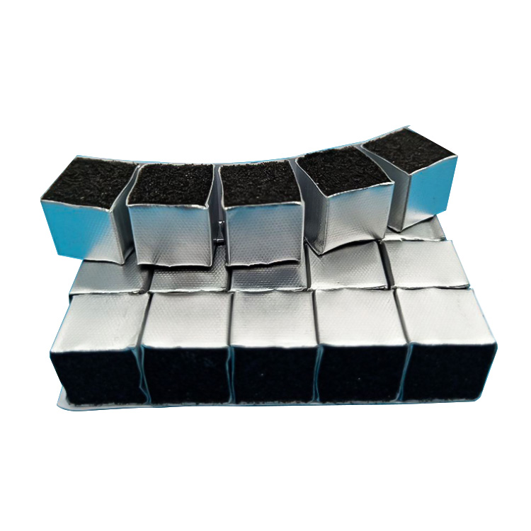
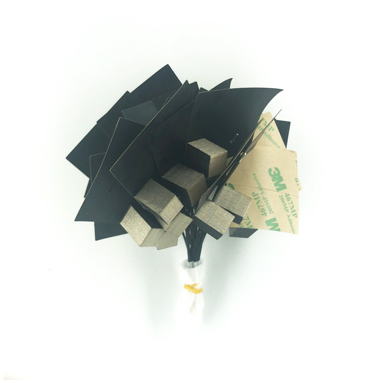
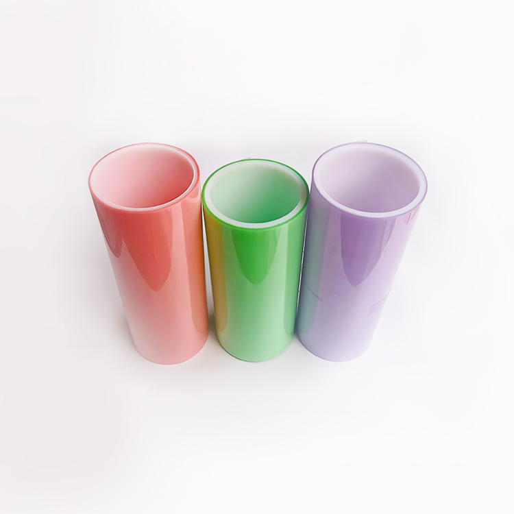
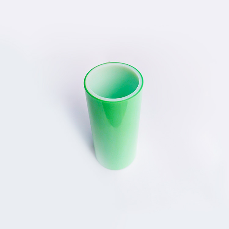
Xinst 6011 Semiconductor Wafer Mounter dicing Tape single sided thermal release tape

* Adhesive strength becomes almost “zero” by heating and REVALPHA can be removed without damaging substrates.
* Substrates can be processed by temporarily fixing a REVALPHA’s pressure sensitive adhesive face to the stage.
* Provides a high processing accuracy since substrates are kept in a fixed position.
*Three types (rolls, labelers and sheets) are available.
* Environmentally friendly since no cleaning is required for substrates

Xinst 6011 Semiconductor Wafer Mounter dicing Tape single sided thermal release tape

Pyrolysis thinning film, called positioning slitting styrofoam in the industry, also known as hot peeling tape/cutting film/mlcc cutting film, etc., before being heated, it is pasted on the surface of the object, which can play a good role in the object. The function of protection and shielding can be easily debonded after the thermal process, so that the processed parts can be easily/easy peeled off without leaving residual glue, which is conducive to automation, saves manpower/material resources, and improves efficiency.

Thermal Release Tape Applications:

Used in delicate and fragile wafer processing; positioning and cutting in the process of MLCC chip capacitors and chip inductors; semiconductor wafer surface processing; electronic and optoelectronic industrial components manufacturing and processing engineering; LCD and TP touch panel glass thinning, grinding and polishing; LED cutting, grinding and polishing; sapphire substrate thinning and polishing process; copper substrate graphene (Graphene) transfer and carbon nanotube transfer applications, which can replace UV blue film.

Size: 150*150 160*160 180*180 200*200mm, etc., special specifications can be cut according to customer needs.

Viscosity: low viscosity 200G; medium viscosity 400G; high viscosity 700G; special viscosity can be customized according to customer needs.

Stripping temperature: 90-100 degrees, the slitting temperature does not exceed 70 degrees; 120-130 degrees, the slitting temperature does not exceed 90 degrees; 140-150 degrees, the slitting temperature does not exceed 120 degrees. Special needs customer demand production.

Foaming peeling time: 10 seconds-3 minutes.

Special reminder; the oven temperature must reach the set temperature before the product can be put in for foaming, so that the effect can be achieved.

Die cutting designs can includes holes, shapes, oversized lines (for easy removal) and complimentary products can also be incorporated.
Die cutting tapes enable you to save a significant amount of time when applying the adhesive tape and to save money for cuts through slitting.


Our Factory Competitive Advantages:

Well Competitive Prices and High Quality Control Prompt Delivery Earth-friendly Products In a Variety of Design Small Order Acceptable OEM Accepted

Roll Size: 3″ paper or plastic core;tape width: 2mm -1200mm; standard width: 1200mm,standard length:50M

OEM Size:Special length, thickness or combinations can be supplied per customer’s request.Products can be supplied in roll,tape,sheets or shapes per customer’s request.Only you provide the CAD drawing,we can die cut any size for you.

Shelf Life: To obtain best performance, use this product within 12 months from date of delivery and store under normal conditions of 60 ºC to 80ºF (16 ºC to 27ºC) and 40 to 60% R.H. in the original carton

Xinst 0611 Semiconductor Wafer Mounter dicing Tape single sided thermal release tape

If the Xinst 6011 Semiconductor Wafer Mounter dicing Tape single sided thermal release tape to your requirement, please be free to buy the quality products made in China with our professional manufacturers and suppliers in China. We’re equipped with a productive factory at your service.

Applications:

Used in delicate and fragile wafer processing; positioning and cutting in the process of MLCC chip capacitors and chip inductors; semiconductor wafer surface processing; electronic and optoelectronic industrial components manufacturing and processing engineering; LCD and TP touch panel glass thinning, grinding and polishing; LED cutting, grinding and polishing; sapphire substrate thinning and polishing process; copper substrate graphene (Graphene) transfer and carbon nanotube transfer applications, which can replace UV blue film.

Size: 150*150 160*160 180*180 200*200mm, etc., special specifications can be cut according to customer needs. Viscosity: low viscosity 200G; medium viscosity 400G; high viscosity 700G; special viscosity can be customized according to customer needs. Stripping temperature: 90-100 degrees, the slitting temperature does not exceed 70 degrees; 120-130 degrees, the slitting temperature does not exceed 90 degrees; 140-150 degrees, the slitting temperature does not exceed 120 degrees. Special needs customer demand production. Foaming peeling time: 10 seconds-3 minutes. Special reminder; the oven temperature must reach the set temperature before the product can be put in for foaming, so that the effect can be achieved.Die cutting designs can includes holes, shapes, oversized lines (for easy removal) and complimentary products can also be incorporated.
Die cutting tapes enable you to save a significant amount of time when applying the adhesive tape and to save money for cuts through slitting.
Product Name
Xinst 0611 Semiconductor Wafer Mounter dicing Tape single sided thermal release tape
Adhesive Type
Foaming adhesive
Color
white/blue/yellow
Temperature Resistance
-20°C -130°C
Before foaming
4.0N/20mm
After foaming
0.02N/20mm
Features

* Adhesive strength becomes almost “zero” by heating and REVALPHA can be removed without damaging substrates.

* Substrates can be processed by temporarily fixing a REVALPHA’s pressure sensitive adhesive face to the stage.
* Provides a high processing accuracy since substrates are kept in a fixed position.
*Three types (rolls, labelers and sheets) are available.
* Environmentally friendly since no cleaning is required for substrates.
Thickness
0.15mm

SEND EMAIL TO US

    email Contact
    go top